Semiconductor Machines Explained: Types, Components, Functions, and Manufacturing Applications
Semiconductor machines are specialized equipment used to manufacture semiconductor devices, including microprocessors, memory chips, sensors, and power-control components. These devices are found in computers, smartphones, vehicles, industrial robots, medical equipment, and communication systems. Semiconductor manufacturing combines materials science, chemistry, physics, electronics, and precision engineering to create extremely small structures on silicon wafers.
Context
Semiconductor machines are specialized equipment used to manufacture semiconductor devices, including microprocessors, memory chips, sensors, and power-control components. These devices are found in computers, smartphones, vehicles, industrial robots, medical equipment, and communication systems. Semiconductor manufacturing combines materials science, chemistry, physics, electronics, and precision engineering to create extremely small structures on silicon wafers.
The development of semiconductor machinery followed advances in electronic components during the twentieth century. As integrated circuits became more complex, manufacturers required equipment capable of creating smaller features, depositing thin material layers, removing unwanted material, and inspecting structures with high precision. Modern semiconductor machines perform these tasks in controlled environments where temperature, particles, pressure, and chemical conditions must be carefully managed.
Understanding Semiconductor Manufacturing
A semiconductor chip begins with a wafer, usually made from highly purified silicon. Manufacturing involves a series of processes that create patterns and electronic structures on the wafer before individual chips are separated, packaged, and tested.
Semiconductor machines are designed for specific stages of this process. Some form patterns on a wafer, others deposit or remove material, and additional equipment checks dimensions, electrical properties, and possible defects. Several machines may be used repeatedly as a wafer moves through the production process.
Main Components of Semiconductor Machines
Although equipment designs differ, many semiconductor machines contain similar functional components:
Wafer handling systems: Move wafers between processing positions while reducing contamination and physical damage.
Process chambers: Enclosed spaces where deposition, etching, or other controlled processes take place.
Optical systems: Direct or measure light during lithography, inspection, and alignment.
Vacuum systems: Maintain reduced pressure for processes that require controlled gas environments.
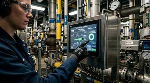
Control systems: Coordinate machine movements, process settings, sensors, and operating sequences.
Measurement sensors: Monitor factors such as temperature, pressure, gas flow, and alignment.
Cleanroom interfaces: Help transfer wafers between equipment and controlled manufacturing areas.
These components work together to maintain repeatable processing conditions. Their design depends on the machine's purpose, the materials being processed, and the precision required.
Importance
Semiconductor machines are important because modern electronic products depend on reliable, compact, and energy-efficient chips. Computers use processors and memory devices, vehicles rely on electronic control units and power semiconductors, and factories use chips in automation equipment, communication systems, and monitoring devices.
Manufacturing equipment also influences production quality, throughput, and the types of chips that can be produced. Errors during processing can create defects across multiple devices on a wafer, making process control and inspection essential. Manufacturers therefore combine specialized machinery with software, measurement systems, and controlled production environments.
Major Types of Semiconductor Machines
Different semiconductor machines perform distinct tasks throughout wafer fabrication and chip testing.
Lithography machines transfer circuit patterns onto a light-sensitive material called photoresist. Optical lithography uses light to create patterns, while extreme ultraviolet lithography uses shorter-wavelength light for certain advanced manufacturing processes.
Deposition equipment adds thin layers of material to a wafer. Chemical vapor deposition and physical vapor deposition use different methods to form films with specific electrical, chemical, or physical properties. Atomic layer deposition can build extremely thin layers through controlled surface reactions.
Etching machines remove selected material from a wafer. Dry etching uses gases or plasma, while wet etching uses liquid chemicals. The selected method depends on the material, pattern, and required shape.
Ion implantation equipment introduces selected atoms into semiconductor materials to change their electrical characteristics. These controlled changes help form regions that allow transistors and other components to function.
Cleaning equipment removes particles, chemical residues, and unwanted material between processing stages. Cleaning methods may use liquids, gases, or other controlled techniques.
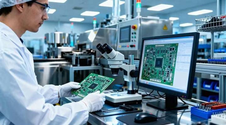
Inspection and metrology systems examine patterns, dimensions, alignment, surface conditions, and defects. Metrology focuses on measurement, while inspection identifies irregularities that may affect device performance.
Packaging and testing equipment handles completed dies, connects them to external electrical contacts, protects them in packages where applicable, and checks their operation.
Comparison of Semiconductor Machine Types
| Machine type | Main function | Typical manufacturing stage |
|---|---|---|
| Lithography system | Transfers circuit patterns | Pattern formation |
| Deposition machine | Adds thin material layers | Layer formation |
| Etching system | Removes selected material | Pattern shaping |
| Ion implantation system | Changes material electrical properties | Device formation |
| Cleaning equipment | Removes contamination and residues | Multiple stages |
| Inspection system | Detects surface and pattern defects | Process monitoring |
| Metrology equipment | Measures dimensions and alignment | Process monitoring |
| Testing equipment | Checks electrical operation | Wafer test and final test |
The exact equipment sequence depends on the chip design, manufacturing technology, and materials involved.
How Semiconductor Machines Work Together
Semiconductor fabrication generally follows a repeated sequence rather than a single uninterrupted operation. A wafer may receive a material layer, undergo coating and lithography, have selected areas etched, and then be cleaned and measured. Many layers and patterning cycles may be needed to create a complete integrated circuit.
Automation coordinates wafer movement, process recipes, and equipment monitoring. Manufacturing software records process information and helps operators identify deviations from defined limits. Even with automation, engineers and technicians remain important for equipment maintenance, calibration, process development, and quality analysis.
Recent Updates
Semiconductor manufacturing equipment continues to evolve as demand grows for artificial intelligence computing, high-performance processors, advanced memory, automotive electronics, and power-management devices. Developments across 2024–2026 have included continued investment in advanced lithography, more complex chip integration, improved inspection methods, and manufacturing approaches designed to manage increasingly demanding device structures.
Advanced Lithography and Process Control
Extreme ultraviolet lithography is used in some advanced semiconductor production lines to create very small circuit patterns. Its operation involves specialized light sources, reflective optical systems, precise wafer positioning, and tightly controlled environments. Equipment complexity and manufacturing requirements limit its use to particular production applications.
Other lithography systems remain important for many chips, including power devices, sensors, microcontrollers, and mature integrated circuits. Semiconductor manufacturing does not rely on one machine type or one technology node for every product.
Advanced Packaging and Chip Integration
Advanced packaging combines multiple semiconductor dies or chiplets within a single package. This approach can connect computing, memory, and specialized processing components while supporting different design and manufacturing requirements. Equipment used in this area includes precision bonding systems, die placement tools, package inspection machines, and electrical testing systems.
Inspection and metrology are also becoming increasingly important as chip structures grow more complex. Manufacturers use advanced measurement methods to examine alignment, material layers, bonding quality, and defects that may not be visible through ordinary optical inspection.
Automation and Equipment Efficiency
Manufacturers increasingly use software analytics, automated material handling, and equipment sensors to monitor production conditions. Data analysis can help identify process variation, equipment wear, and maintenance needs. Results depend on data quality, machine design, and the way these systems are integrated into factory operations.
Laws or Policies
Semiconductor machines are affected by industrial safety rules, environmental requirements, export controls, and government policies supporting semiconductor manufacturing. Applicable requirements depend on the machine, its technology, its destination, and the activities performed at a facility.
Semiconductor Manufacturing Policy in India
India's semiconductor development initiatives include the India Semiconductor Mission and the Semicon India programme. The national semiconductor programme supports activities such as semiconductor fabrication, display manufacturing, assembly, testing, marking, and packaging, subject to the relevant scheme requirements and approvals.
These initiatives are intended to develop domestic manufacturing capabilities and strengthen the semiconductor supply chain. Eligibility, financial support, and implementation conditions depend on the specific programme and its current guidelines. Industrial projects must also meet applicable land-use, building, environmental, and operational requirements.
Safety, Environmental Rules, and Export Controls
Semiconductor manufacturing can involve hazardous chemicals, specialized gases, high temperatures, radiation sources, and high-voltage equipment. Facilities must follow applicable occupational safety, chemical handling, waste management, and environmental rules. Specific obligations depend on the processes and materials used.
International trade rules can also affect semiconductor machinery. Certain advanced equipment, software, and technical items may be subject to export licensing or restrictions under the laws of the exporting country and relevant trade-control frameworks. Requirements can change according to technology specifications, destination, and end use.
Tools and Resources
Technical resources help readers understand semiconductor equipment, manufacturing stages, and industry developments. Different resources focus on engineering principles, equipment specifications, policy information, or general market knowledge.
Technical Learning Resources
The Semiconductor Industry Association publishes information about semiconductor technology and the wider industry. SEMI provides industry standards, technical resources, and information related to semiconductor manufacturing equipment and factory operations. The websites of equipment manufacturers can also explain lithography, deposition, etching, inspection, and wafer handling.
University materials and engineering textbooks provide background on semiconductor physics, integrated circuits, and fabrication methods. These sources help explain why particular machines are needed and how individual processes contribute to chip formation.
Manufacturing and Process Tools
Several tools support semiconductor equipment design and operation:
Process simulation software: Models selected fabrication processes or material behavior.
Computer-aided design tools: Help engineers design chip layouts and supporting equipment components.
Statistical process control software: Tracks manufacturing measurements and identifies variation.
Equipment monitoring dashboards: Display machine status, sensor readings, alarms, and process records.
Metrology systems: Measure dimensions, film thickness, alignment, and other process characteristics.
These tools serve different purposes and may require specialized training. Their capabilities depend on the software, equipment configuration, and manufacturing process.
FAQs
What are semiconductor machines used for?
Semiconductor machines manufacture and inspect chips used in electronics, vehicles, communication systems, industrial automation, and computing devices. They perform tasks such as pattern formation, material deposition, etching, cleaning, and testing.
What are the main types of semiconductor manufacturing equipment?
Major types include lithography machines, deposition systems, etching equipment, ion implantation machines, cleaning systems, inspection tools, metrology equipment, and chip testing machines. Each performs a specific role in the manufacturing sequence.
How do semiconductor lithography machines work?
Lithography machines transfer circuit patterns onto a light-sensitive coating on a wafer. The developed pattern guides later processing steps, including material removal or selective layer formation.
Why are inspection machines important in semiconductor manufacturing?
Inspection machines identify defects, particles, and pattern irregularities that may affect chip quality. Metrology equipment measures dimensions and process characteristics to help manufacturers maintain production controls.
What semiconductor manufacturing initiatives exist in India?
India's semiconductor initiatives include the India Semiconductor Mission and the Semicon India programme. These support domestic semiconductor manufacturing and related activities under specific eligibility requirements and government guidelines.
Conclusion
Semiconductor machines perform specialized tasks that transform semiconductor wafers into electronic components. Lithography, deposition, etching, cleaning, inspection, and testing equipment work together throughout the manufacturing process. Recent developments in advanced lithography, packaging, automation, and measurement reflect the growing complexity of chip production. Industrial safety rules, environmental requirements, trade controls, and government initiatives also influence how semiconductor equipment is developed and used.