Advanced Chip Packaging Equipment Guide: Processes, Tools, Materials and Manufacturing Methods
An Advanced Chip Packaging Equipment Guide explains the processes, tools, materials, and manufacturing methods used to assemble semiconductor chips into reliable electronic components. Semiconductor manufacturing involves creating tiny electronic circuits on silicon wafers, but these circuits must also be protected, electrically connected, and integrated with other components. Chip packaging performs these functions and helps connect a semiconductor device to a circuit board or a larger electronic system.
Context
An Advanced Chip Packaging Equipment Guide explains the processes, tools, materials, and manufacturing methods used to assemble semiconductor chips into reliable electronic components. Semiconductor manufacturing involves creating tiny electronic circuits on silicon wafers, but these circuits must also be protected, electrically connected, and integrated with other components. Chip packaging performs these functions and helps connect a semiconductor device to a circuit board or a larger electronic system.
Traditional semiconductor packages often contain a single chip connected to a supporting substrate or lead frame. Advanced chip packaging extends these methods through technologies that place multiple chips together, create dense electrical connections, or stack components vertically. These approaches are increasingly relevant to processors, memory devices, artificial intelligence hardware, telecommunications equipment, and other computing systems.
Understanding Advanced Chip Packaging
Advanced packaging combines mechanical assembly, electrical interconnection, thermal management, and protective materials. Unlike front-end wafer fabrication, which creates transistors and circuits, packaging focuses on connecting and protecting the completed semiconductor structures.
Several packaging methods are used in modern manufacturing:
Flip-chip packaging: A chip is connected to a substrate through small conductive bumps or pillars rather than conventional wire connections alone.
Fan-out packaging: Electrical connections extend beyond the original chip footprint through a redistribution layer.
2.5D packaging: Multiple chips are connected through an interposer or another high-density interconnection structure.
3D packaging: Semiconductor dies are stacked vertically to shorten connections or combine different functions.
Chiplet integration: Separate functional chip sections are assembled into one package, allowing different components to be developed or manufactured using different processes.
Each approach has different requirements for alignment, interconnection density, materials, heat removal, and inspection.
Main Equipment Used in Packaging
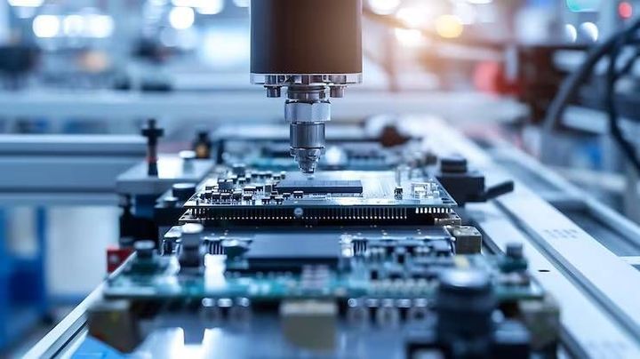
Advanced chip packaging equipment performs specialized tasks at different stages of production. Common equipment includes die bonders for positioning semiconductor dies, flip-chip bonders for precise alignment, wire bonders for connecting chips with fine wires, and molding systems for applying protective compounds.
Other equipment includes wafer thinning machines, dicing systems, redistribution-layer processing tools, substrate handling systems, thermal compression bonding equipment, and inspection instruments. A manufacturing line combines these tools according to the package design, material selection, production volume, and required quality controls.
Importance
Advanced chip packaging matters because the performance of an electronic system depends on more than the transistors inside its processors. Electrical connections, power delivery, signal transmission, heat removal, and physical reliability can all affect how a device operates.
As computing workloads grow, packaging can help integrate processing units, memory, and specialized accelerators within a compact assembly. This is particularly relevant to artificial intelligence systems, high-performance computing, data centers, automotive electronics, and advanced communication equipment.
Manufacturing Challenges and Practical Applications
Manufacturers must address several challenges when assembling small, densely connected semiconductor structures. Tiny alignment errors, material expansion, surface contamination, uneven bonding, or trapped voids can affect electrical connections and package reliability.
Thermal management is another important concern. High-performance chips can generate substantial heat, and tightly integrated packages may make heat removal more difficult. Engineers therefore evaluate package geometry, thermal interface materials, heat spreaders, cooling arrangements, and power distribution during design and production.
Advanced packaging also affects manufacturing planning. Equipment selection influences process accuracy, throughput, inspection requirements, maintenance schedules, and compatibility with existing production facilities. Engineers, equipment operators, materials specialists, and quality teams all contribute to controlling the packaging process.
Comparing Packaging Methods
The table summarizes common technologies and their general characteristics.
| Packaging method | Main approach | Important consideration |
|---|---|---|
| Wire bonding | Fine wires connect the die to package contacts | Wire placement and connection reliability |
| Flip-chip | Conductive bumps connect the die to a substrate | Alignment and bump integrity |
| Fan-out | Redistribution layers extend electrical connections | Layer accuracy and material stability |
| 2.5D integration | Multiple dies connect through an interposer or similar structure | Interconnect density and thermal design |
| 3D stacking | Dies are stacked vertically | Heat removal and vertical connections |
| Chiplet integration | Separate functional dies are combined | Interface compatibility and system integration |
These methods are not interchangeable in every application. The appropriate process depends on electrical requirements, package dimensions, thermal limits, materials, and manufacturing constraints.
Recent Updates
From 2024 through 2026, advanced chip packaging has received increased attention as semiconductor manufacturers develop hardware for artificial intelligence, high-performance computing, and high-bandwidth memory. Industry activity has focused on increasing integration density, improving manufacturing yield, and expanding the capacity of packaging facilities. The pace of adoption varies according to technology, production readiness, and supply-chain conditions.
Hybrid Bonding and High-Density Interconnections
Hybrid bonding is an interconnection method that joins prepared surfaces using direct metal-to-metal connections alongside dielectric bonding. It can support very fine connection spacing in suitable applications, including certain three-dimensional integration approaches. Its implementation requires careful surface preparation, cleanliness, alignment, and process control.
Thermal compression bonding is also used in advanced packaging. It applies controlled heat and pressure to establish connections between dies and substrates. Equipment must maintain accurate alignment and appropriate bonding conditions to reduce defects.
Chiplets and High-Bandwidth Memory
Chiplet designs allow semiconductor systems to combine separate dies with different functions. For example, a package may contain processing components, input/output circuitry, and memory interfaces. This approach can provide design flexibility, although it introduces requirements for compatible electrical interfaces, testing, and thermal management.
High-bandwidth memory uses vertically stacked memory dies and dense connections to support data-intensive computing. Packaging equipment used in these systems may include precision die placement, wafer thinning, stacking, bonding, and advanced inspection tools. Manufacturers continue to refine these processes as package complexity increases.
Automation, Inspection, and Process Monitoring
Packaging facilities increasingly use automated material handling, machine vision, equipment monitoring, and process data analysis. These systems can help identify alignment deviations, track process conditions, and detect defects at different manufacturing stages.
However, automation does not remove the need for engineering validation. Equipment performance depends on calibration, material consistency, maintenance, process design, and the accuracy of inspection methods.
Laws or Policies
Advanced chip packaging equipment is affected by semiconductor manufacturing standards, workplace safety requirements, environmental rules, intellectual property protections, and international trade controls. The exact requirements depend on the equipment, materials, destination, and intended application.
Semiconductor Manufacturing Policy in India
India's semiconductor policy framework includes the India Semiconductor Mission and government initiatives intended to develop domestic semiconductor manufacturing and related supply-chain capabilities. The broader policy environment covers semiconductor fabrication, assembly, testing, marking, and packaging activities, subject to the terms and eligibility requirements of particular programs.
Government support arrangements may change, and participation depends on applicable guidelines, approvals, and project conditions. A packaging facility's regulatory obligations also depend on its location, construction, equipment, and manufacturing processes.
Safety and Environmental Requirements
Packaging equipment may involve high temperatures, moving machinery, vacuum systems, chemicals, gases, and electrical hazards. Facilities must assess relevant occupational safety requirements, provide appropriate training, and establish procedures for handling materials and maintaining equipment.
Environmental rules may apply to chemical storage, wastewater, air emissions, electronic waste, and the disposal of process materials. In India, applicable central and state regulations can include environmental protection, factory safety, and hazardous-waste requirements, depending on the activity.
Export Controls and Technical Standards
Certain semiconductor equipment, components, and related technologies may be subject to export controls or licensing requirements. Restrictions depend on technical specifications, destination, end use, and applicable national rules. Businesses involved in international shipments must assess the rules relevant to each transaction.
Industry standards and internal qualification procedures also support consistent manufacturing. These may cover materials, electrical testing, reliability testing, contamination control, and process documentation. Compliance with a particular standard depends on the product, customer requirements, and applicable regulatory framework.
Tools and Resources
Technical resources help readers understand equipment functions, process compatibility, and semiconductor packaging developments. Useful references include industry organizations, equipment documentation, research publications, and manufacturing process diagrams.
Industry References and Technical Learning
SEMI publishes industry standards and information relevant to semiconductor manufacturing equipment, materials, and facilities. The IEEE Electronic Packaging Society provides technical publications and educational resources related to electronic packaging, interconnections, and thermal management.
The Institute of Electrical and Electronics Engineers (IEEE) Xplore digital library contains research papers on chiplets, 2.5D integration, 3D stacking, bonding technologies, and package reliability. Academic institutions and semiconductor research centers also publish material explaining packaging processes and emerging techniques.
Equipment Evaluation and Process Planning
A packaging equipment comparison spreadsheet can organize technical requirements across different machine types. Useful fields include die-size range, alignment capability, bonding method, substrate compatibility, process temperature, throughput, inspection capability, maintenance needs, and facility requirements.
Process flow diagrams help explain how equipment is connected across a production line. A simplified workflow may include wafer preparation, thinning, dicing, die placement, interconnection, encapsulation, testing, and final inspection. Actual process sequences vary by packaging technology.
Inspection and Reliability Tools
Optical microscopes, automated optical inspection systems, X-ray inspection, scanning acoustic microscopy, and electrical test equipment can identify different types of defects. For example, X-ray imaging can help examine internal connections, while acoustic inspection can reveal certain internal separations or voids.
No single inspection method detects every defect. Manufacturers combine suitable inspection and testing methods based on package construction, known failure mechanisms, and reliability requirements.
FAQs
What is advanced chip packaging equipment?
Advanced chip packaging equipment includes machines used to position, connect, stack, protect, and inspect semiconductor dies. Examples include die bonders, flip-chip bonders, wafer thinning tools, molding systems, and inspection equipment.
What materials are used in advanced chip packaging?
Common materials include silicon, organic substrates, copper, solder alloys, dielectric materials, molding compounds, underfill materials, and thermal interface materials. Selection depends on electrical, mechanical, thermal, and manufacturing requirements.
How does 2.5D packaging differ from 3D chip packaging?
In 2.5D packaging, multiple dies are generally placed side by side and connected through an interposer or similar structure. In 3D packaging, dies are stacked vertically, often requiring dense vertical interconnections and careful thermal management.
Why is hybrid bonding used in semiconductor packaging?
Hybrid bonding can create dense electrical connections between prepared surfaces and support advanced die integration. It requires precise alignment, clean surfaces, and tightly controlled manufacturing conditions.
What factors matter when evaluating chip packaging equipment?
Important factors include package type, die dimensions, alignment accuracy, bonding technology, material compatibility, throughput, inspection capability, maintenance, and production requirements. Equipment must match the process and package design.
Conclusion
Advanced chip packaging equipment supports the assembly of semiconductor dies into compact, electrically connected, and mechanically protected packages. Technologies such as flip-chip bonding, fan-out packaging, chiplet integration, and three-dimensional stacking address different integration requirements. Recent developments emphasize dense interconnections, thermal management, automation, and process inspection. Manufacturing policies, safety requirements, technical standards, and export controls also influence how packaging equipment is developed and used.